A roughly $10,000 GPU with 40GB of memory ought to demolish a gaming card, right?
Well, that depends entirely on what you ask it to do. The NVIDIA A100 is a monster built for artificial intelligence, high performance computing, and enormous datasets. Ask it to render a Blender scene, and an RTX 3090 can embarrass it. Give it a suitable machine learning workload, though, and suddenly the price tag starts making a lot more sense.
NVIDIA doesn’t normally seed these cards to reviewers, and buying one just to mess around with wasn’t exactly an easy expense to justify. Fortunately, someone offered to lend us one. Their identity stays private, but the deal was simple: test Ethereum mining, build a cooling shroud, and put the thing back together before returning it.
Yes, that meant we could take it apart. Obviously, we took it apart.
Table of Contents
- Key Takeaways
- What Makes the A100 Different?
- Under the Shroud: A Familiar Face
- Getting a Server GPU Running on an Open Test Bench
- Blender: The RTX 3090 Fights Back
- Can the A100 Run Games?
- Ethereum Mining: Fast, but This Was Never a Buying Recommendation
- Folding@home: Efficiency Is Easier to Establish Than a Winner
- ResNet-50: Finally, an A100 Workload
- The Real Lesson: Buy for the Workload, Not the Price Tag
Key Takeaways
- The A100 excels at specialized compute, not every task that benefits from a powerful GPU.
- The RTX 3090 won both Blender tests, with a much larger lead using OptiX.
- ResNet-50 throughput reached roughly 2,400 images per second at about 250W on the A100.
- Running a passive server accelerator on a desktop requires deliberate airflow, compatible power, and suitable firmware settings.
What Makes the A100 Different?
Our sample was the NVIDIA A100 PCIe 40GB, not the higher power SXM module intended for specialized server platforms. Even within the A100 family, those distinctions matter.
Here are the important specifications for the card we tested:
- GPU: GA100, manufactured on TSMC’s 7nm process.
- CUDA cores: 6,912.
- Core clocks: 765MHz base and up to 1,410MHz boost.
- Memory: 40GB of HBM2.
- Memory interface: 5,120 bits.
- Memory bandwidth: Approximately 1.5TB/s.
- Power budget: 250W.
Forty gigabytes sounds ridiculous next to a consumer graphics card, but it can still be restrictive for the datasets these accelerators process. By the time of our test, an 80GB A100 was already available.
The NVLink connectors along the top edge let compatible systems link multiple accelerators for communication and larger, coordinated workloads. That is a very different world from installing one card to make games go faster.
For context, we had two useful comparison points. The CMP 170HX mining accelerator looked suspiciously similar to the A100 physically. For performance, we used an MSI RTX 3090 Suprim, since we didn’t have an RTX A6000 available. This wasn’t a professional workstation certification comparison, so the 3090 was a useful stand-in for exploring how a powerful consumer GPU handles the same tasks.
Under the Shroud: A Familiar Face
Remove the gold-colored outer shell, and the A100 looks remarkably like the CMP 170HX. Both use a long passive heatsink, a similar clamshell construction, and no display outputs.
That last point is not an oversight. This is a compute accelerator, not a gaming card that happens to be missing an HDMI connector.
There is another important omission inside GA100: the video encoding hardware found on chips such as the RTX 3090’s GA102. This is not simply an encoder hidden by a driver setting. The hardware is not there.
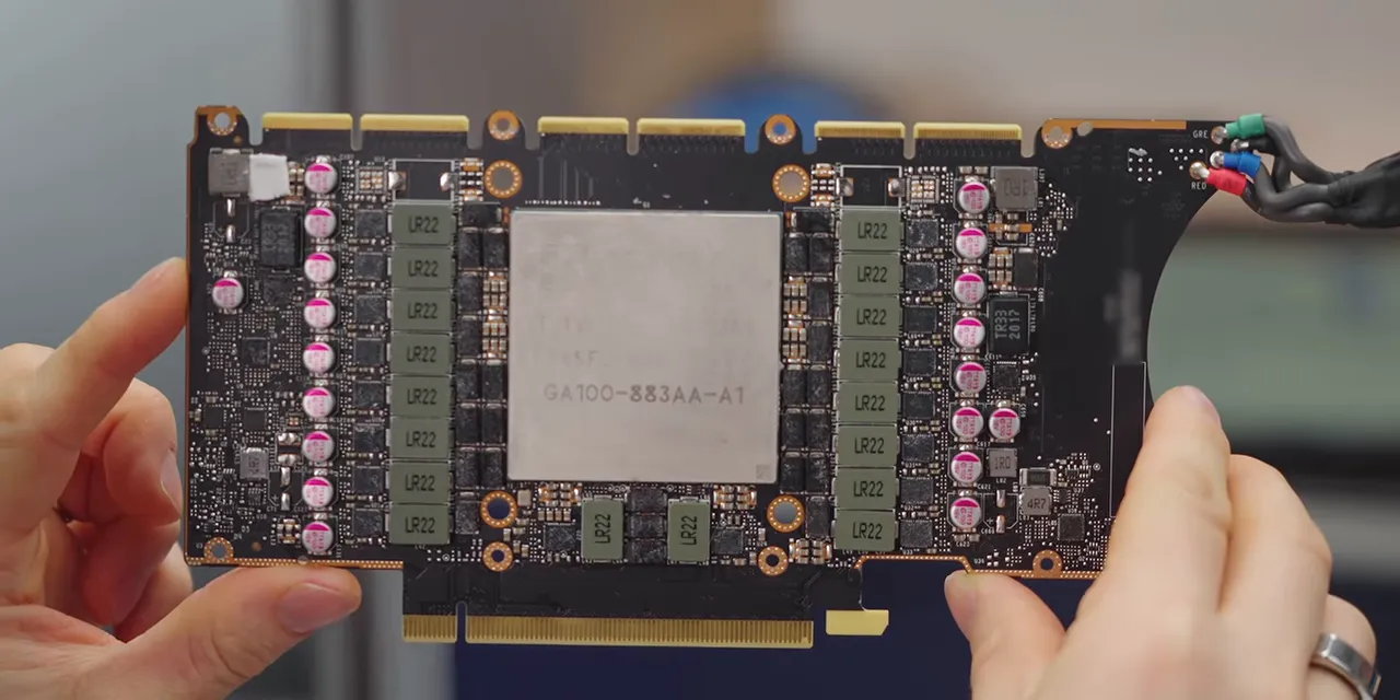
That Eight-Pin Connector Is Not What You Think
The power connection deserves special attention. The A100 uses an eight-pin EPS-style connector, rather than the familiar eight-pin PCIe GPU connector.
A normal PCIe power plug would not fit. A CPU-style EPS plug matched the connector, although the retaining clips interfered somewhat in our demonstration. The server-oriented power arrangement can also use the appropriate adapter fed by two PCIe connectors.
The practical lesson is simple: eight pins do not make two power connectors interchangeable. Use the correct wiring and adapter for the card, not whichever cable looks close enough.
Similar Hardware Does Not Mean Identical Capabilities
With the cooler removed, the A100’s large integrated heat spreader became visible. The resemblance to the CMP card continued, but that did not establish that the two products had identical functionality.
The CMP has less memory and a restricted PCIe connection, and its NVLink connections are not accessible for normal use. We also found different chip markings. Some third-party CMP specifications raised questions, but those were not enough to draw firm conclusions about the exact functional units enabled on each chip.
NVIDIA has long sold products based on related silicon with different capabilities enabled through hardware configuration and software. The important distinction is between what exists physically on a chip and what a particular product actually exposes.
The SXM A100 is another reminder not to generalize too aggressively. Its packaging differs, and the version we discussed had a roughly 400W power budget rather than our PCIe card’s 250W. Same family, different operating conditions.
After cleaning the heat spreader, applying fresh thermal paste, and reassembling the card, it was time to find out whether we still owned a functioning loaner.
Getting a Server GPU Running on an Open Test Bench
The A100 has no fan. It is essentially one enormous heatsink with a vapor chamber underneath to spread heat from the GPU.
In a server, that makes sense. The chassis supplies substantial airflow through the card. On an open desktop test bench, it means you need to provide that airflow yourself. Passive cooling does not mean the card can run under load without forced air.
Jake’s solution was a 3D-printed fan duct, affectionately called the Shroudinator. It attaches to the mounting holes normally used to secure the back of the card in a server and lets us mount a fan at the end.
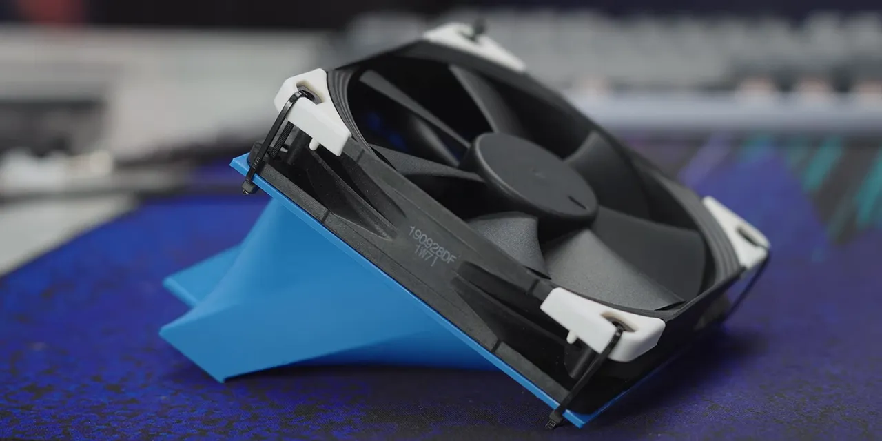
Was it the pinnacle of aerodynamic engineering? Absolutely not. Back pressure pushed some air out where we didn’t particularly want it. Was it enough to cool the card for our testing? Yes.
The fan duct print file is available for anyone working on a similar setup.
BIOS Settings and Driver Oddities
The system did not boot successfully with the A100 installed right away. On our platform, getting it working required:
- Enabling Above 4G Decoding in the BIOS.
- Changing an additional MMIO address-space setting to 42.
- Keeping another GPU installed to provide display output.
That MMIO detail is a report of what worked on our motherboard, not a universal BIOS recipe. Firmware labels and available settings vary.
We installed the RTX 3090’s Game Ready driver and NVIDIA’s data center driver. There appeared to be some overlap or replacement between the packages, but both cards were usable for the tasks we tried.
One oddity: the A100 did not appear in Windows Task Manager’s GPU performance section. That did not stop compute applications from using it. Task Manager is not the final authority on whether a data center accelerator is working.
Blender: The RTX 3090 Fights Back
We chose Blender’s Classroom scene because the smaller BMW render would finish too quickly on an RTX 3090 to make a particularly useful comparison.
In CUDA mode, the results were surprisingly close:
- RTX 3090: 1 minute, 18 seconds.
- A100: 1 minute, 22 seconds.
So, yes, the extremely expensive enterprise accelerator was slower. Not catastrophically slower, but slower.
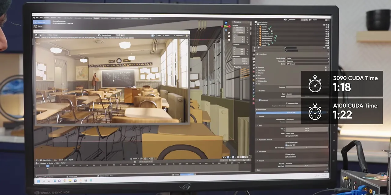
The power consumption made things more interesting. We observed the A100 drawing around 150W during rendering, compared with roughly 350W on the 3090. Comparable completion times at substantially lower power is worth noticing, even when the cheaper card wins outright.
OptiX Makes the Hardware Difference Obvious
Switching to OptiX changed the story dramatically:
- RTX 3090: Approximately 36 seconds.
- A100: Approximately 1 minute, 14 seconds.
The 3090 was now about twice as fast.
The A100 has fewer CUDA cores than the 3090, and crucially, it has no dedicated RT cores. OptiX could still run on the A100, but that did not magically give it the ray tracing acceleration present in the gaming GPU.
Tensor cores can contribute to supported AI denoising, but they do not replace RT cores for the rest of the rendering workload. Our interpretation was that the A100 was relying on its general compute path for that work, while the 3090 could use hardware specifically suited to ray tracing.
For more background on those rendering backends, the Blender GPU rendering documentation explains the available options.
The result is a useful reality check: an enterprise GPU is not automatically the best GPU for every professional application.
Can the A100 Run Games?
We tried Windows’ per-application graphics selection to see whether we could assign a game to the A100 and send the resulting image through another GPU.
No luck. Windows would not offer the A100 as a gaming GPU in that setup.
GPU-Z helped explain why. We could identify compute support such as CUDA and OpenCL, but the tested configuration exposed no usable DirectX support, and Vulkan was not shown as supported either. Checking the DirectX 12 information produced a device-not-found result.
GPU-Z also showed some other capability flags, including OpenGL and PhysX, but those were not evidence that ordinary Windows gaming would work. We did not establish a functioning alternative gaming path.
In short, this was not going to be another clever conversion of a headless mining card into a bargain gaming GPU. Also, at about $10,000, “bargain” was already doing some heroic work.
Ethereum Mining: Fast, but This Was Never a Buying Recommendation
The lender specifically asked for an Ethereum mining test, so we ran one. These are historical proof-of-work results, not a present-day Ethereum mining guide.
The A100 managed roughly 175MH/s at 250W, with efficiency around 714kH per watt in one observed reading. That was broadly similar to the CMP 170HX’s mining performance and substantially faster than the 3090 result we were discussing.
For comparison, a tuned RTX 3090 could deliver around 120MH/s at 300W. The A100’s memory bandwidth clearly had something useful to do here.
Tuning options were limited. We could adjust the core clock and reduce the power limit, but could not change memory speed through the available controls. Lowering the power limit improved efficiency somewhat while reducing throughput.
Impressive? Sure. A sensible reason to buy an A100 at its original price? That is an entirely different question.
Folding@home: Efficiency Is Easier to Establish Than a Winner
Our Folding@home experiment came with a major qualification: the server assigns different work units, and those jobs can reward different numbers of points per day.
That makes a short comparison between two GPUs less conclusive than a controlled benchmark. One card can appear faster simply because it received a more favorable job. Our comparison tool also showed the 3090 running roughly 31% below its average, which reinforced the need for caution.
The A100 appeared competitive, but we could not responsibly turn that brief run into a definitive performance ranking.
The power difference, however, was hard to miss:
- RTX 3090: Approximately 400W.
- A100: Approximately 240W.
That is why performance per watt keeps coming up. In a desktop, another hundred watts may feel like a secondary consideration. In a data center full of accelerators, power delivery and cooling become major parts of the infrastructure and operating cost.
Consider eight 400W SXM accelerators in one chassis, then multiply that across dozens of chassis. Suddenly, efficiency is not a footnote. It is a design requirement.
ResNet-50: Finally, an A100 Workload
Enough asking an AI accelerator to do everything except AI.
For machine learning testing, we switched to Ubuntu because the benchmark stack we wanted to use was better suited to Linux. We set up the CUDA Toolkit and drivers, Docker, and NVIDIA’s container tooling to run a ResNet-50 benchmark in TensorFlow 2.
Both cards used the same key settings:
- XLA: Enabled.
- Batch size: 512.
- Precision: FP16 rather than FP32.
- Accelerators per test: One GPU.
We monitored power and memory usage with NVIDIA System Management Interface, or nvidia-smi. It is NVIDIA’s command-line management and monitoring utility, and it gave us the telemetry Windows Task Manager was not providing.
The RTX 3090 Was Already Seriously Fast
The 3090 filled its 24GB of VRAM and averaged 1,435 images per second. That is a substantial result for a consumer gaming card doing a machine learning workload.
The catch was power: we observed approximately 412W.
The A100 Delivered More While Drawing Less
Running the same test on the A100 filled its 40GB of memory and produced roughly 2,400 images per second. Power consumption was about 250W.
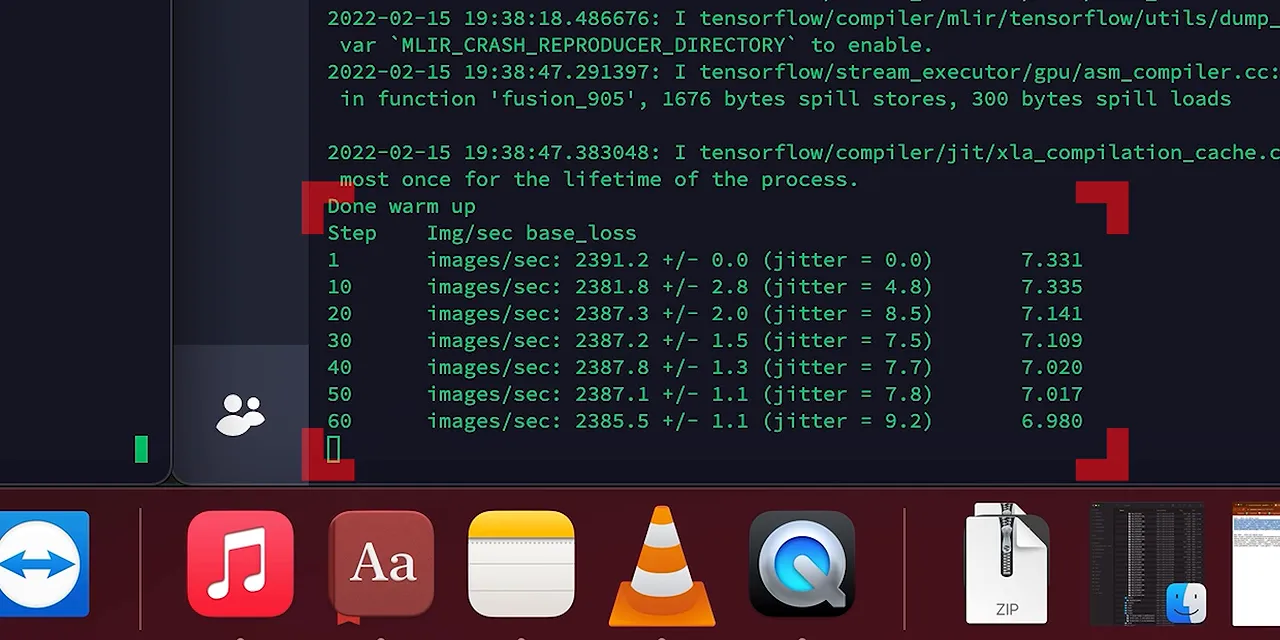
That is around 1,000 additional images every second while using substantially less power. Holy bananas.
Using those approximate throughput and power figures, the A100 delivered about 1.7 times the performance and roughly 2.7 times the throughput per watt. That calculation applies to this particular test, not every AI model or deployment.
But this is where the product finally makes sense. Not as an absurdly expensive gaming card. Not as an automatic Blender champion. As a specialized compute accelerator doing the work it was designed to do.
The Real Lesson: Buy for the Workload, Not the Price Tag
The A100’s results were almost comically dependent on the application. It narrowly lost our CUDA render, lost badly in OptiX, refused our Windows gaming experiment, delivered strong historical mining performance, and then showed exactly why it belongs in a machine learning server.
“Most expensive” and “fastest for my application” are not synonyms. Neither are CUDA core counts, memory bandwidth, or a shared architecture enough to predict the winner on their own.
The other exciting part was seeing Ampere on TSMC’s 7nm process, compared with the Samsung 8nm process used for NVIDIA’s contemporary gaming lineup. Process-node names from different manufacturers are not directly comparable, and our results do not isolate manufacturing process from all the other architectural differences. Still, the efficiency was impressive.
At the time, reports suggested that the upcoming Ada Lovelace gaming architecture would move to a newer TSMC process. That made the A100 feel like an encouraging glimpse of what better efficiency might enable, not proof of how an unreleased gaming card would perform.
For our everyday work, an A100 was mostly an opportunity to experiment with hardware we would never sensibly buy. For the right data center workload, though, it was an absolute monster. Just make sure the workload is right, the power cable is right, and someone has plugged in the fan.


